
Ordering number : ENN7245
20703AS (OT) No. 7245-1/4
Overview
The STK412-000 series are class H audio power amplifier
hybrid ICs that feature a built-in Shift power supply
circuit. These ICs provide high efficiency audio power
amplification by controlling (switching) the supply
voltage supplied to the power transistors according to the
detected level of the input audio signal.
Features
∑ Pin compatible IC series that covers power ratings from
50 W
◊
2 channels to 180 W
◊
2 channels at 0.7 or 0.8%
THD, 20 Hz to 20 kHz. This allows the use of a
common PCB for all output classes.
∑ The pin arrangement is also unified with that of the
three-channel STK413-000 series. This means that PCBs
designed for three-channel models can also be used for
two-channel models.
∑ Miniature package
-- 50 W/ch to 120 W/ch (THD = 0.8%, f = 20 Hz to 20
kHz): 64
◊
36.5
◊
8.5 mm*
-- 150 W/ch to 180 W/ch (THD = 0.7%, f = 20 Hz to
20 kHz): 78
◊
44
◊
9 mm*
* Not including the IC pins.
∑ Allowable load shorted time: 0.3 s
Package Dimensions
unit: mm
4196-SIP18
1
18
64.0
55.6
18.7
36.5
(6.21)
17
◊
2.54=43.18
3.6
0.5
2.54
8.5
4.0
0.4
5.5
25.8
2.9
SANYO: SIP18
[STK412-010]
STK412-010
SANYO Electric Co.,Ltd. Semiconductor Company
TOKYO OFFICE Tokyo Bldg., 1-10, 1 Chome, Ueno, Taito-ku, TOKYO, 110-8534 JAPAN
Two-Channel Shift Power Supply Audio Power Amplifier ICs
70W + 70 W
Thick-Film Hybrid IC
Any and all SANYO products described or contained herein do not have specifications that can handle
applications that require extremely high levels of reliability, such as life-support systems, aircraft's
control systems, or other applications whose failure can be reasonably expected to result in serious
physical and/or material damage. Consult with your SANYO representative nearest you before using
any SANYO products described or contained herein in such applications.
SANYO assumes no responsibility for equipment failures that result from using products at values that
exceed, even momentarily, rated values (such as maximum ratings, operating condition ranges, or other
parameters) listed in products specifications of any and all SANYO products described or contained
herein.
No. 7245-2/4
STK412-010
Parameter
Type No.
STK412-090
STK412-000
STK412-010
STK412-020
STK412-030
STK412-040
STK412-150
STK412-170
Output (20 Hz to 20 kHz)
50 W + 50 W
60 W + 60 W 70 W + 70 W
80 W +80 W 100 W + 100 W 120 W + 120 W 150 W + 150 W 180 W + 180 W
[THD]
[0.8 %]
[0.8 %]
[0.8 %]
[0.8 %]
[0.8 %]
[0.8 %]
[0.7 %]
[0.7 %]
Maximum supply voltage, V
H
±60 V
±65 V
±69 V
±73 V
±80 V
±84 V
±95 V
±95 V
(No signal)
Maximum supply voltage, V
L
±41 V
±42 V
±44 V
±45 V
±46 V
±51 V
±61 V
±60 V
(No signal)
Recommended supply voltage,
±37 V
±39 V
±43 V
±45 V
±51 V
±54 V
±57 V
±54 V
V
H
Recommended supply voltage,
±27 V
±29 V
±30 V
±32 V
±34 V
±36 V
±38 V
±37 V
V
L
Recommended load impedance
8
6
4
Package
64 mm
◊
36.5 mm
◊
8.5 mm
78 mm
◊
44 mm
◊
9 mm
Series Organization
Parameter
Symbol
Conditions
Ratings
Unit
V
H
: Maximum supply voltage 1 (no signal)
V
H
max(1)
±69
V
V
H
: Maximum supply voltage 2 (signal present)
V
H
max(2)
R
L
= 8, 6
±62
V
V
H
: Maximum supply voltage 3 (signal present)
V
H
max(3)
R
L
= 4
±49
V
V
L
: Maximum supply voltage 1 (no signal)
V
L
max(1)
±44
V
V
L
: Maximum supply voltage 2 (signal present)
V
L
max(2)
R
L
= 8, 6
±40
V
V
L
: Maximum supply voltage 3 (signal present)
V
L
max(3)
R
L
= 4
±30
V
V
H
-V
L
: Maximum supply voltage
*
4
V
H-L
max
No load
60
V
Thermal resistance
j-c
Per power transistor
1.9
∞C/W
Junction temperature
Tj max
Both the Tjmax and Tcmax conditions must be met.
150
∞C
Operating IC substrate temperature
Tc max
125
∞C
Storage temperature
Tstg
≠30 to +125
∞C
Allowable load shorted time
*
3
ts
V
H
= ±43 V, V
L
= ±30 V, R
L
= 8
, f = 50 Hz, P
O
= 70 W,
0.3
s
one channel operating
Specifications
Maximum Ratings
at Ta = 25∞C
These products are organized into a series based on their output power.
Parameter
Symbol
Test conditions
*
1
Standard value
Unit
V
CC
(V)
f (Hz)
P
O
(W)
THD (%)
min
typ
max
P
O
(1)
V
H
= ±43
20 to 20 k
0.8
70
W
Output power
V
L
= ±30
P
O
(2)
V
H
= ±34
1 k
0.8
R
L
= 4
70
W
V
L
= ±25
Total harmonic distortion
THD
V
H
= ±43
20 to 20 k
70
0.4
%
V
L
= ±30
Frequency characteristics
f
L
, f
H
V
H
= ±43
1.0
+0 ≠3 dB
20 to 50 k
Hz
V
L
= ±30
Input impedance
ri
V
H
= ±43
1 k
1.0
55
k
V
L
= ±30
Output noise voltage
*
2
V
NO
V
H
= ±52
Rg = 2.2 k
1.0
mVrms
V
L
= ±34
Quiescent current
I
CCO
V
H
= ±52
No load
30
mA
V
L
= ±34
No load
100
mA
Midpoint voltage
V
N
V
H
= ±52
≠70
0
+70
mV
V
L
= ±34
Operating Characteristics at Ta = 25∞C, R
L
= 8
, Rg = 600
, VG = 40 dB, V
Z
= 15 V, R
L
must be a non-
inductive load.
Notes:
*
1. Unless otherwise specified, a constant-voltage power supply must be used during inspection.
*
2. The output noise voltage rating gives the peak value read by an averaging VTVM. However, to eliminate the influence of flicker noise from the AC
primary side line, use an AC stabilized power supply (50 Hz).
No. 7245-3/4
STK412-010
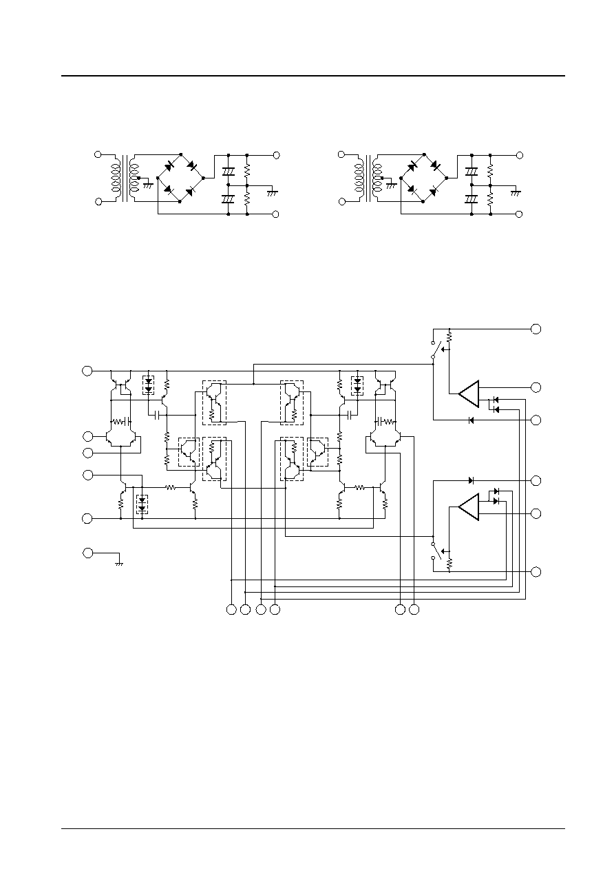
Internal Equivalent Circuit
TR3
TR6
TR2
TR1
R2
TR7
R7
R3
C2
C1
R6
R1
TR5
TR4
13
15
9
16
12
8
11
10
17
18
TR9
TR10
R4
R5
TR8
D1
D2
TR13
TR16
TR12
TR11
TR41
R12
R41
R13
R14
R15
C12
C11
TR17
R17
R16
R11
TR15
TR51
TR14
TR18
TR19
TR20
D12
D41
D51
D53
D52
D42
D43
1
2
5
4
6
14
Comparator
R51
Comparator
3
SUB
7
10000
µ
F
10000
µ
F
DBA40C
500
500
+VH
--VH
+
+
10000
µ
F
10000
µ
F
DBA40C
500
500
+VL
--VL
+
+
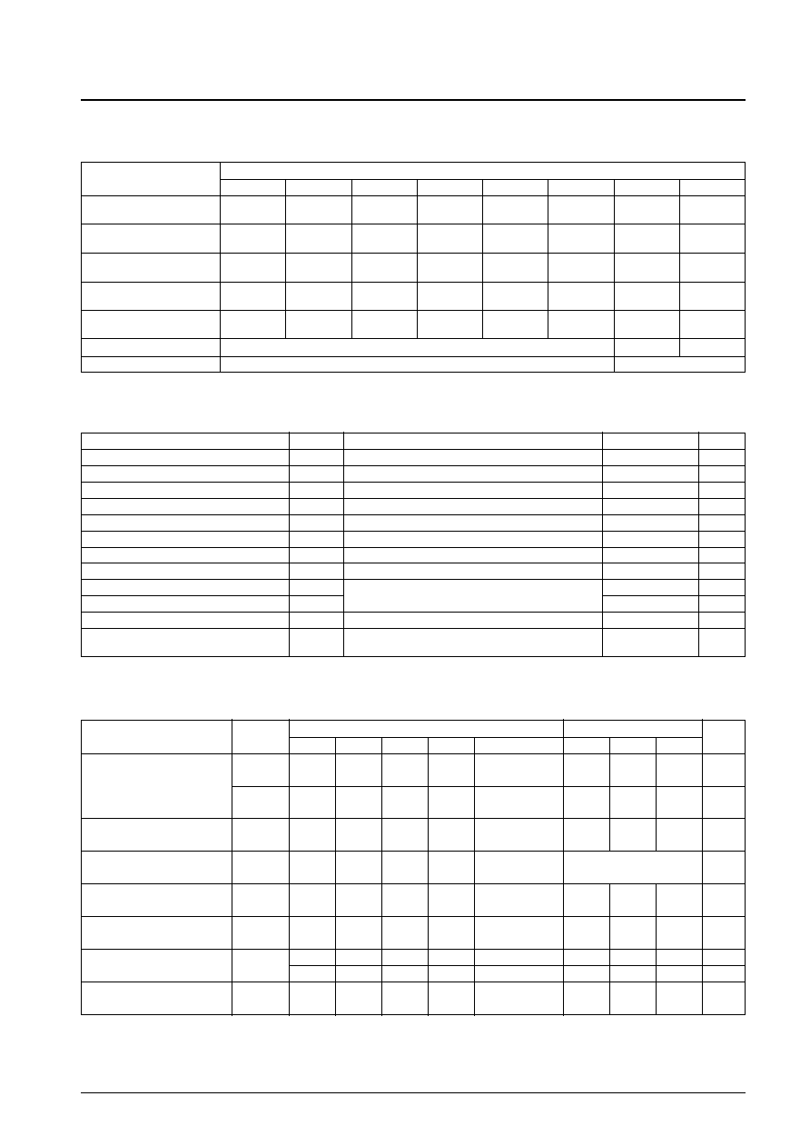
Specified Transformer Power Supply
(MG-250 equivalent)
Specified Transformer Power Supply
(MG-200 equivalent)
*
3. Use the transformer power supply specified in the figure below for allowable load shorted time and output noise voltage measurements.
*
4. Design circuits so that (|V
H
| - |V
L
|) is always less than 40 V when switching the power supply with the load connected.
*
5. Set up the V
L
power supply with an offset voltage at power supply switching (V
L
- L
O
) of about 8 V as an initial target.
PS No. 7245-4/4
STK412-010
This catalog provides information as of February, 2003. Specifications and information herein are subject
to change without notice.
Specifications of any and all SANYO products described or contained herein stipulate the performance,
characteristics, and functions of the described products in the independent state, and are not guarantees
of the performance, characteristics, and functions of the described products as mounted in the customer's
products or equipment. To verify symptoms and states that cannot be evaluated in an independent device,
the customer should always evaluate and test devices mounted in the customer's products or equipment.
SANYO Electric Co., Ltd. strives to supply high-quality high-reliability products. However, any and all
semiconductor products fail with some probability. It is possible that these probabilistic failures could
give rise to accidents or events that could endanger human lives, that could give rise to smoke or fire,
or that could cause damage to other property. When designing equipment, adopt safety measures so
that these kinds of accidents or events cannot occur. Such measures include but are not limited to protective
circuits and error prevention circuits for safe design, redundant design, and structural design.
In the event that any or all SANYO products (including technical data, services) described or contained
herein are controlled under any of applicable local export control laws and regulations, such products must
not be exported without obtaining the export license from the authorities concerned in accordance with the
above law.
No part of this publication may be reproduced or transmitted in any form or by any means, electronic or
mechanical, including photocopying and recording, or any information storage or retrieval system,
or otherwise, without the prior written permission of SANYO Electric Co., Ltd.
Any and all information described or contained herein are subject to change without notice due to
product/technology improvement, etc. When designing equipment, refer to the "Delivery Specification"
for the SANYO product that you intend to use.
Information (including circuit diagrams and circuit parameters) herein is for example only; it is not
guaranteed for volume production. SANYO believes information herein is accurate and reliable, but
no guarantees are made or implied regarding its use or any infringements of intellectual property rights
or other rights of third parties.
Sample Application Circuit
33k
1
2
3
4
5
6
7
8
9
10
11
12
13
14
15
16
17
18
STK412-000 Series
GND
GND
560
100
µ
F
/100V
100
µ
F
/100V
100
µ
F
/50V
100
µ
F
/50V
100
µ
F
/63V
100
µ
F
/63V
2.2
µ
F
/50V
2.2
µ
F
/50V
470pF
100pF
100pF
470pF
0.1
µ
F
560
100
µ
F
/10V
100
µ
F
/10V
3pF
*
1
*
1
*
1
*
1 56k
1.5k
/1W
1.5k
/1W
GZA
15X
GZA
15X
100
/1W
100
/1W
3pF
56k
1k
1k
Ch.2 IN
56k
56k
Ch.1 IN
Ch.1 OUT
Ch.2 OUT
3
µ
H
3
µ
H
4.7
4.7
4.7
/1W
0.1
µ
F
4.7
/1W
SUB.GND
--VL
+VH
--VH
+VL
GND
*
1: Cement resistor, 0.22
, ±10% (5 W)